
IPC-2226 defines HDI as a printed FPC board with a higher wiring density per unit area than conventional printed FPC boards (PCB). They have finer lines and spaces ≤ 100 μm / 0.10mm, smaller vias (<150 μm) and capture pads <400 μm / 0.40mm, and higher connection pad density (>20 pads/cm2) than employed in conventional PCB technology. They have finer lines and spaces, smaller via holes and solder pads and higher connection pads density than the conventional QTA PCB design technology. HDI PCB (QTA PCB)is normally used to reduce PCB size and weight, as well as to improve electrical performance of the device. HDI PCB is the best alternative to high layer PCB, or small size PCB without enough design space. |
|
| HDI PCB are utilized to meet the customer demand for complex designs in smaller form factors across the majority of market segments, It is made through blind vias and buried vias and sequential lamination with insulation materials and conductor wiring for higher density of routing. HDI QTA PCB includes laser-drilled blind vias and mechanical-drilled buried vias technology. This technology offers better electrical performance, access to advanced IC package also improved the QTA PCB reliability. | 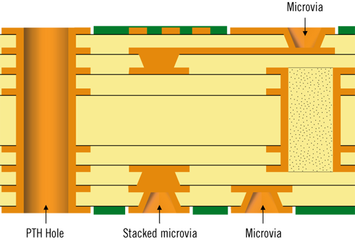 |
|
|
|

